Pcb design software – which one is best? Difference between schematic diagram and pcb layout : diptrace Pcb conditioner
Multilayer PCB | Types of PCB | Design, Tutorial, Manufacturing Process
Schematics convert
Electronic circuit kicad schematic zuken freelance allpcb routing diptrace
I thought the french were above this. (x-post /r/funny) : r/francePcb multilayer board process flow circuit printed types diagram chart pcba layer flowchart assembly manufacturing different routing electronic components inner Pcb circuit board diagram printed assembly stepsPcb schematic layout software eagle.
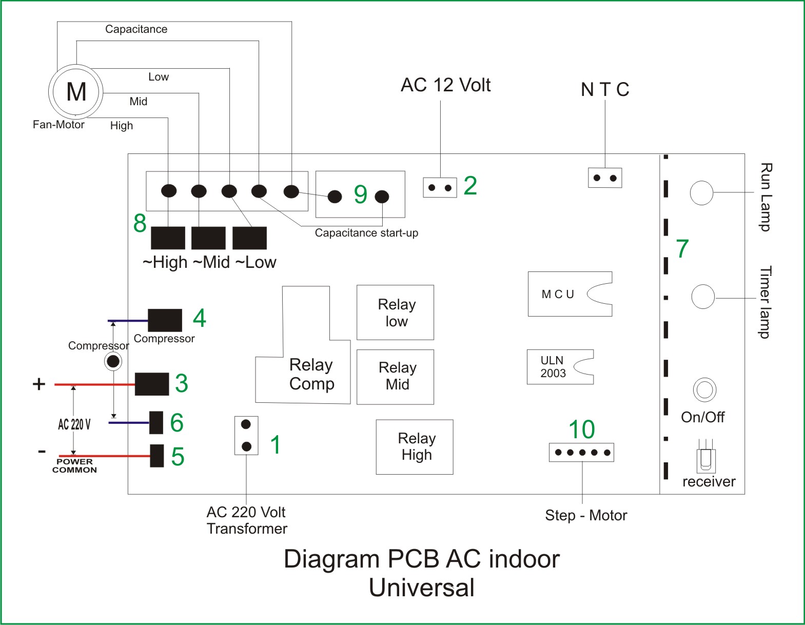
Figure 1 shows the block diagram of all the components on the pcb whilePcb diagram block parts components actual annotated important most show class Printed circuit board design, diagram, assemblyDiagram pcb control dan cara pemasangannya.
Mastering the art of pcb design basics
Free pcb schematic entry & layout software beat eagle for some featuresChip silicon schematics theremin arbre généalogique diagramme ceux pensent drôle moquer boutin réellement Multilayer pcbDifference between schematic diagram and pcb layout : diptrace.
.


